Make your first schematic
This article is part three in the series about taking your project from idea to finished product. Previous article described how to make a concept. Now, lets take that concept and make a schematic from it!
My preferred program suite for electronics design is KiCAD, a free and open source EDA that runs on Windows, Mac and Linux. There are other program suites and which one you use will not matter much for this article. So, start your program of choice and create a project.
Table of Contents
Where to start?
When you have created your project and opened the schematic capture tool you are met with a blank screen. Getting from a blank screen to this

Can seem a bit overwhelming at the start, and my Servercooler project is a relatively simple device. To make it more approachable we will utilize the block diagram created in the previous step. KiCAD is a hierarchical tool, which means that the main sheet can contain subsheets in a hierarchy. This design philosophy maps quite well with the block diagram approach. Other tools might work differently so don't get too hung up on this detail
Component choices
I think it is a good idea to start choosing the main components. Main components are the big building blocks you can see on a PCB, and they provide most or all of the function of a specific block. The types of components are things like
- Power supply ICs
- Transistor drivers
- Power transistors
- MCUs
- Driver ICs
- Amplifiers
and so many more it is hard to list them all. It is usually a good idea to choose these first as they usually drive other design choices by having requirements of supporting components and signals. So lets choose some main parts!
MCU
The MCU had a few requirements that needed to be fulfilled
- Minimum 1 timer with input capture
- Minimum 1 timer with PWM generation
- Minimum hardware UART
- "Enough" GPIO
- STM32 Series
- A sensible package for soldering
I did actually choose the MCU quite late in the project. I knew which series and type of processor but I needed to do some design work to find out how much GPIO I needed. There are also requirements to keep track of regarding program memory and RAM, but at the level of programming I am doing it is usually not a concern. The chosen MCU is quite basic and still has a massive 12kB SRAM and serviceable 32 kB of program flash.
Power supply
Current consumption
Open a spreadsheet editor or bring out your calculator. It is time to start calculating a lot. The most important factor for the power supply are
- Input voltage
- Output voltages
- Output current rating
- Regulating performance
open a web-browser and browse to your favourite electronics distributor. I have mostly used Digikey, but you can use others such as Mouser.
The starting point for the powersupply is to determine what its main requirements are. From the block diagram step we already know these factors
- Input voltage = 12V
- Output voltages, 5V and 3.3V
What we are missing is the output current. In the previous guide we already decided that the 3.3V should be created from the DCDC converted 5V, so lets start with summerizing the 3.3V loads. The loads are
- ESP8266
- The MCU
- Pull up resistors
- Indicator LEDs
The ESP8266 module I am going to use datasheet says that the maximum power is used when transmitting, which is around 215mA. Then there is the MCU. In the MCU datasheet you can see the current need is stated in a quite obnoxious manner. There is a lot of information that is not really necessary if you are not planning to do a very lower power device with features permanently disabled. In this project, we will care about the maximum power at rated speed. This mean add all the currents for peripherals together and multiply the current/MHz with the rated speed and add this on top of the core current consumption. I would suggest to also round the numbers up liberally to get some margin in the design. With all this, the current consumption is
43.56 * 48 = 2064 uA
for the peripherals. The numbers are taken from table 35 in the datasheet. The core current consumption is found in table 30 and is 3.75mA under worst conditions, for a total of just under 7mA for the core. As can be seen, this MCU use quite little power.
Then there are resistors and LEDs. The pull-up resistors use around 0.3 - 3 mA at the absolutely worst case. The LEDs are assumed to use around 5mA each for a total sum of maybe 30mA for all small resistors and LEDs. Our 3.3V total is now at ~255mA. Lets round that to 0.5A to have margin for fan switching currents and any missed consumers and small peaks.
As for 5V consumption. The 5V should supply the entire 3.3V current consumption on top of its own loads. The 5V load is only the level shifter with its very small consumption of under 1 mA. This puts the total 5V consumption at basically the same 500mA as the 3.3V. The last current consumer is the fans 12V outputs. They are rated at 1A each and it should be possible to use them at full power at the same time for a total of 4A.
The last part is calculating 12V current use by the DC-DC converter. Assume a 80% efficiency for it. The output power is
3.3*0.5 = 1.65 W
With 80% efficiency that means that the input power is
0.858/0.8 = 2.063 W => 0.172mA
The DCDC part will then also use ~175mA at full output power for a total of 4175 mA. This consumption is important for the reverse polarity protection.
Choose a DCDC converter
Now, lets open that digikey tab again and look for a suitable DCDC converter. This can be quite overwhelming as a beginner (there are 32 300 parts in that category) so filtering is quite important. We can start with setting the output voltage to 5V, minimum input to 12V and the output current to minimum 1A. I generally prefer to keep the max rating of the supply quite a lot higher than 12V. I count on ~14V being a realistic voltage to have, which generally mean the supply need to be able to handle 24V at the maximum. Why this is the case will be explained soon.
Now, the amounts of hits are down to ~9000. Sort the hits on price and start looking for something good. This is quite time consuming, especially the first time you do it. My general advice is
- Get something that has many parts in stock
- Find something with a long datasheet.
- Find something with good examples in the application notes
- Look for a cheap part
Point 1 makes sure the part is not out of stock after your design is finished. The other parts are helpful for design work. A long datasheet might look intimidating, but it beats having a datasheet where things are assumed to be "common knowledge" and not explicitly specified. I am personally is fond of Texas Instruments parts for this reason. Based on these criteria, I chose the TPS5633 from TI. It is a 3A rated DCDC converter supporting up to 28V input so it should be well enough for this.
Now lets do the same for the linear 3.3V regulator, I ended up with the TLV1117LV33 chosen because it requires very small output and input capacitors.
Input protection
The input protection is next. The input protection consist of a TVS diode and a reverse polarity protection MOSFET. The TVS diode is the first choice. It should have these properties
- Standoff voltage min 14V
- 500W peak power
- Max clamping voltage under 28V
I choose the SZ1SMA15CAT3G from littlefuse as it fulfils all my requirements. The choise of this component means that all parts connected directly to the 12V net need to be resistant to ~24V for short times, where "short times" means a few us.
The next part of the input protection is the reverse polarity protection MOSFET. The MOSFET rating is determined by the max current draw. Generally, I want to keep the power dissipation under 0.5W, which at 4.5A mean a max RDSon of 25mOhm.
P = I*I*R = > R = P/(I*I) = 0.5/(4.5*4.5) ~ 0.025 Ohm
I had trouble finding one at an acceptable price point, so I chose one with 34mOhm RDSon. It should still be fine as the power dissipation is under the maximum rated and the max current draw is very unlikely to ever happen to this device. Because of this, the Si2369DS from Vishay was chosen.
Fan high side outputs
The fans will need a circuit for the high side outputs. As explained in the last article, there is no need for high switching performance so the fans will be driven by a PMOS/NMOS combo. These can be purchased as one device, which is what I did. The requirements are not that harsh. 1A and a max power loss of 0.5W was again used as the requirements. The G300C03L6 from Goford was used. It is a 55mOhm FET, so the power loss is well under the limit at 0.055W.
5V control signal
The control signal need to be 5V, which as previously established is a problem. I was looking for a cheap way of doing it and found the SN74HCS125PWR. It is a voltage buffer that has a wide range of voltages. I have now become a bit uncertain if it is actually going to work as I managed to miss that the threshold for input HIGH rise as VCC is increased. It is going to be tight, but we will see. Maybe it will be OK.
That was all the major part choices. Now it is only a question of making the rest of the design.
Schematic design
So now it is time to start making the real schematic. I hope you did not put that calculator away, as now it will become even more useful. I will present the schematic as I designed it, in blocks starting with the input protection.
Input protection block
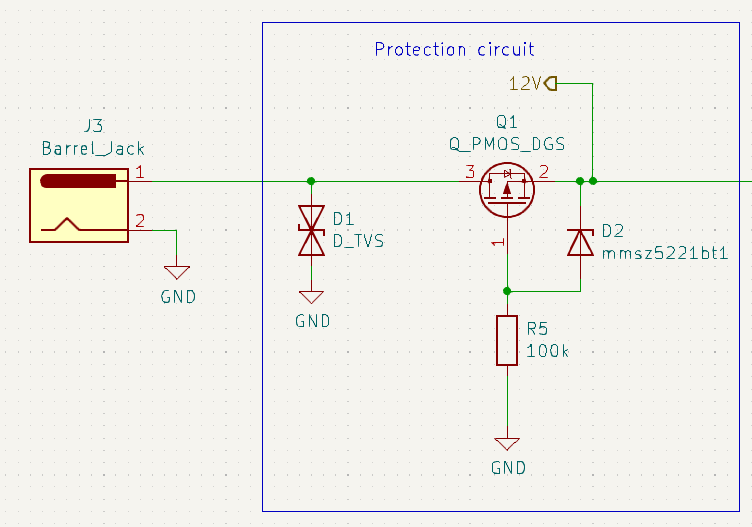
The figure above show the input protection block. D1 is the TVS chosen earlier. Its purpose is to shunt the excessive energy in a voltage transient to ground. The TVS start to conduct some very small amount of current around 15V and this current rises rapidly until it reaches the clamping voltage of 24.4V. The powersupply is rated to 28V so there is some margin. The rest of the components that are connected to the 12V rail also need to deal with up to ~25V.
The next part of the protection block is the PMOS working as an ideal diode. When power is applied, the PMOS will act as a diode through the body diode for a very short time. The voltage on the 12V line rises while the gate on pin 1 stays at 0V. The PMOS will start turn on once the Vgs voltage rises above around 7 or so V, which will lower the losses in the component. If reverse polarity is applied, the Vgs voltage cannot rise while the body diode is reverse biased. This will protect the circuit from any current in the wrong direction. D2 is an optional Zener diode to protect the gate of the PMOS. If the Vgs voltage rises above the breakdown limit for the diode it will start to conduct current and thusly clamp the voltage across it to this limit. D2 is not neccesary for function and if a PMOS with high Vgs max rating is chosen it can be omitted. The Si2369DS used as the ideal diode has a max Vgs of +-20V so D2 will be populated by a Zener diode with around 14 - 16V zener voltage. R5 need to be placed to current limit D2, and its rating is a balancing act between power dissipation and sinking enough current to ensure the diode is working in the rated reverse current zone. To little current and D2 will not clamp, to much current and it will burn up.
Power supply
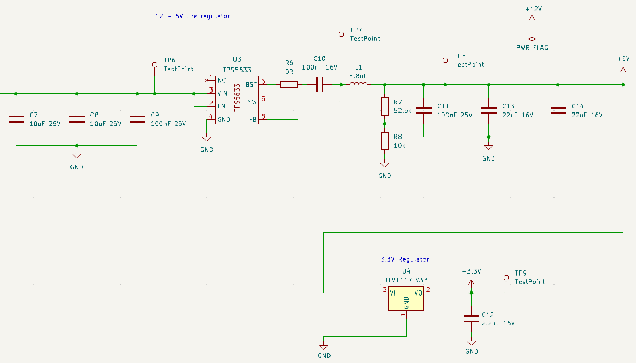
The powersupply circuit is shown above. The DC-DC converter is based on the TPS5633 from Texas Instruments. The supporting components are quite shamelessly stolen from the application notes, with some modification to the inductor to better suit the lower power demand of this device. The very clear and detailed documentation is one of the reasons I chose this IC over some similar ICs that are a bit cheaper. Modern Texas Instrument ICs are just amazing to work with for this reason. I will not show all the calculation needed to adapt the circuitry here as it is a bit to long. Please refer to the excellent datasheet for guidance. Section 8.2.2 even has an example implementation with all calculations needed shown.
The 3.3V power supply is fed by the 5V rail. This IC is a special version of the quite "classic" TLV1117 regulator. The regulator has a very small output capacitance need to the trade-off is that it has a very low input voltage tolerance. The device is rated to only 5.5V, which of course is not a problem here. It does not have many requirements stated apart from input and output capacitance. The input capacitance is provided by the close 5V output caps, and the 2.2uF output cap is taken straight from the datasheet.
I am quite happy with this part. I set out to make the supply reasonably efficient, small and cheap which I think succeeded. The total BOM for the powersupply is around $2.5, where a lot is the capacitors that could be a lot cheaper in slightly larger quantities.
Fan outputs
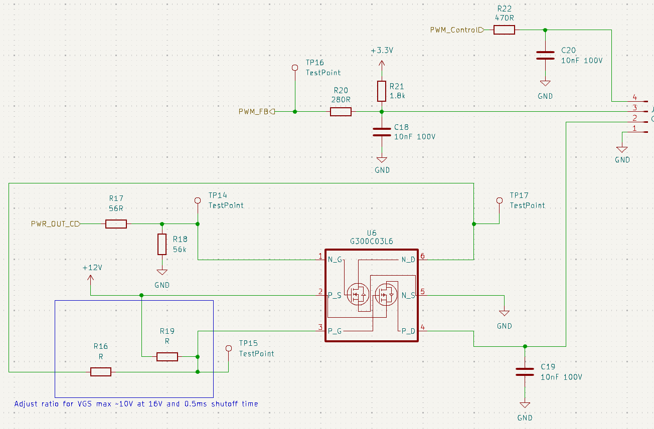
The image above show a fan output, from which there are four identical on the board. The fan output is a pretty simple circuit. It consist of
- The high side output
- The 5V control PWM
- The feedback signal
- A ground return
In this schematic the most complicated part is the high side driver. It is based on an IC that integrate a PMOS and a NMOS. The NMOS is connected to the MCU and a pull down resistor R18 with R17 to current limit the MCU output. The drain of the NMOS is connected to 12V through a pull-up resistor chain which make sure the PMOS is not active as long as the NMOS is off. When the NMOS is on, the PMOS gate is pulled low. R19 and R16 form a resistor divider for which I have not set the ratio yet. The idea is to make sure the PMOS gate is not exceeding the limit even if the 12V rail floats up to 24V for a short moment. The device will work as expected even if R16 is replaced with a zero ohm resistor.
The feedback signal is very simple and lifted from the whitepaper Noctua published. It is a pull up to 3.3V, with a series resistor R20 to the MCU to provide some protection against faults. The MCU inputs are connected to carefully chosen pins on the MCU that can use timers supporting input capture. Why this is the case will be talked about in the software part.
The 5V control signal only show the series protection resistor and ESD suppression capacitor on this page. The 5V translation IC will be shown later so lets leave it for now.
Analogue input
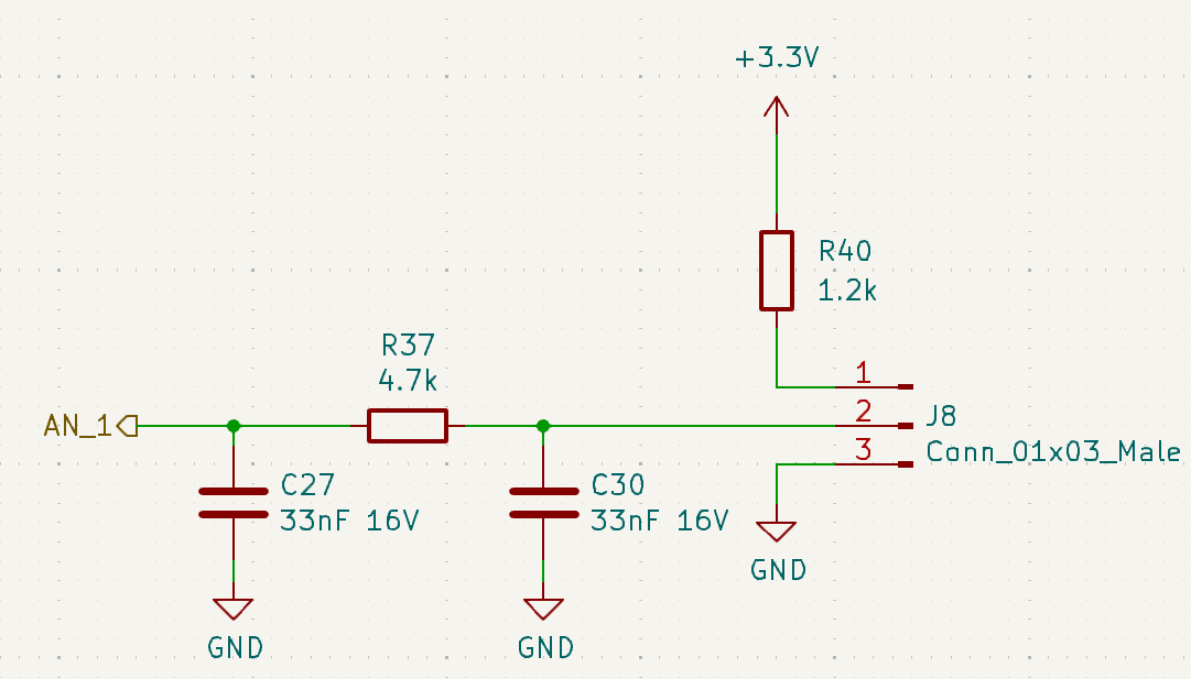
The analogue inputs are also very simple. They have a pull-up to 3.3V to interface with a NTC. Resistor R37 is chosen to provide a reasonable filter of the signal as well as input protection. The idea is that all components does not need to be populated. The input is planned to be able to use DS18D20 temperature probes as an alternative. If that is the case, R40 shall be replaced with a zero ohm resistor while the filters are depopulated. The input to the MCU is here also carefully chosen to be able to use the 1-wire interface. There are 3 of these on the board
ESP8266
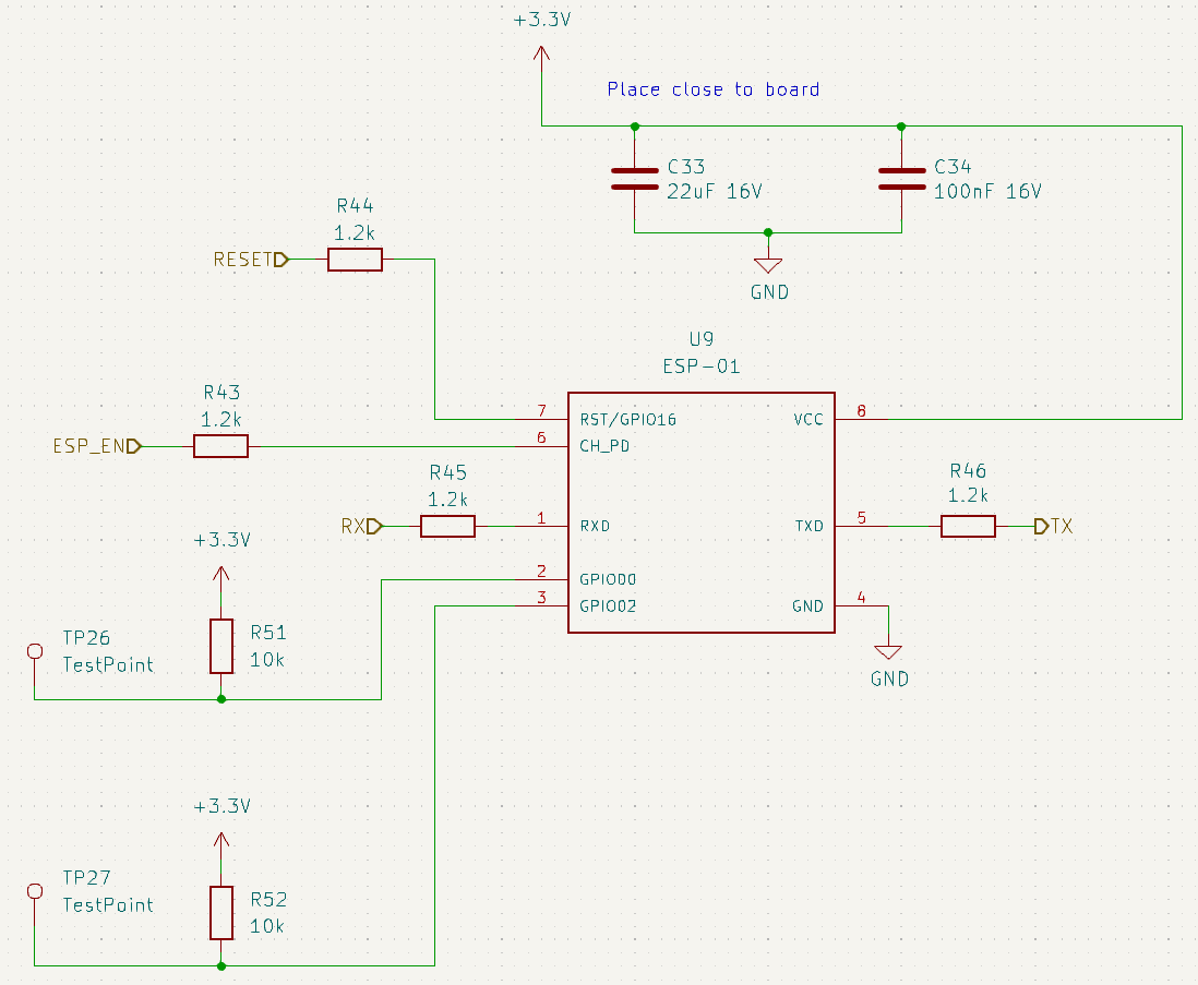
Above is the ESP8266 module with its surrounding circuitry. The supporting circuitry is quite simple as the module is complete as is. The additions is C33 and C34 for additional decoupling that is probably unnecessary. The rest of the resistors are either to give the pins a defined state at startup or to limit the current during switching.
MCU
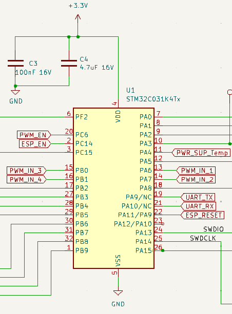
The MCU is the STM32C031K4T6 as described in the last post. The MCU is a cheap 32-bit MCU designed to replace older 8-bit design with more powerful and modern designs. One of the features of being such a low cost device is that there is no external clock required. It can be supplied if it is important that the internal clocks are very accurate, but in this case the internal one should be fine. The decoupling capacitors are taken straight from the recommendations in the datasheet. One big 4.7uF cap for bulk capacitance and then one 100nF to provide a low impedance current source for the fast switching events. Both of these need to be placed very carefully in the layout in the next step. This kind multi capacitor setup is common for MCUs or processors. For faster devices it is common to need several sizes in different package sizes for each supply pin to achieve both the bulk capacitance and low impedance required.
Buttons
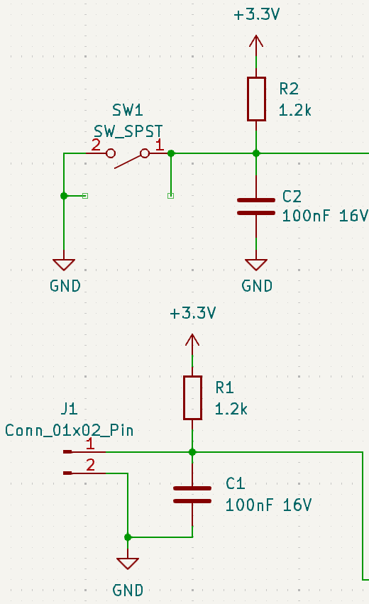
The buttons are shown above. They are quite simple circuits with pull up resistors allowing for basically zero power draw unless pressed. The 100nF capacitor is used to provide a bit of debounce, but there will also be debounce implemented in Software. One of the buttons are on board for the reset pin, and one is connected to a connector for an external button.
Conclusion
So, that was all! Or at least everything that is remotely interesting. I skipped the debug LEDs and debug port for example. The next step is the most fun part, PCB design! Stay tuned until that article is published!