Make your first layout
This post is part four in the series about taking your project idea to a finalised PCB in hand. This time we will talk about making a PCB out of the schematic from part three, or making a layout as you will also often find it mentioned as. Just like last time, I will be using KiCAD but any other EDA will work as well. Some features might just look a bit different or be called something slightly different.
Table of Contents
Where to start this time?
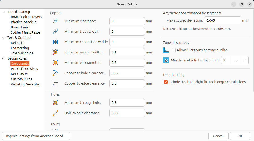
The first step is to decide how the board should be configured. How many layers, copper weights on those layers. Limits for clearance, creepage and minimal features etc. It is also possible to change the properties of the dielectric material. This is quite a long list, but a lot is either probably irrelevant or already chosen for you. Lets start with creepage and dielectric material. If you read this guide you should not need to care about these as it is only relevant for either higher voltages or high frequencies, both of which are not suitable for a first project. Default option will be good
Next we have clearence and minimal features. This is most likely already chosen for you as it is something that the board house has as design constraints because of their process. You can find places where these limits can be changed, but those are most likely not really something anybody reading this will use as they are one or two orders of magnitude more expensive than the ones targeting "hobbyist" or generic prototyping.
Choosing a supplier
For hobbyist there are usually only three things that matters when choosing a supplier.
- Price
- Speed
- Ease of use
The most ones I know as suitable for hobbyist are either JLCPCB, PCBway or oshpark. There might be others, but those are the ones I have checked out. I personally mostly use JLCPCB as it happened to be the one I started with and I am happy with the experience/quality. I understand PCBway is about equal. Oshpark makes little sense to me as it based in the US, which means I get all the shipping/tax annoyances as buying from China for a much higher price. For somebody in the US, they might be a much more sensible choice. So visit them all and check out what makes sense to you
Getting the board setup right
Now it is time to check out what PCBs the chosen supplier can manufacture. It is usually called "capabilities" and will be a long list of constraints/tolerances. Check those out as well as the ordering tool to get a sense for what is free, what is cheap and what is expensive. If you don't know for sure you need something extra, go with the defaults except for layer count. So lets start the PCB layout tool and put all this data into the board stackup. In KiCAD it is called .
How many layers?
One big question is the number of layers you shall use. It is possible to do most designs with any layer count, at least as a general rule. What a higher layer count will do is make it possible to place components much tighter since the space to do signal routing is increased. But it comes at a cost, higher layer counts are usually more expensive. Higher layer counts will also be a bit more confusing in the beginning as you need to keep more things in your head at the same time. For a first project 2 layers are probably going to be what you shall choose, but I would argue that 4 layers is not that dumb for a beginner either. I will be writing this guide mostly assuming 2 layers, and then later show what 4 layers allow you to do.
Start with PCB design
First things first, size and mounting hardware
The first thing to do is to decide on a PCB size. There are two approaches to this in my opinion
- Get the components out and make a guess
- Take the space you have assigned from the project
I have found that most hobbyist projects, at least until you get very ambitious fall into category 1. More advanced projects or professional work will be in category 2. I will assume you have a category 1 situation.
How big are my components now again?
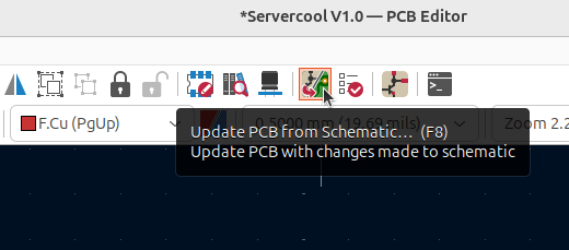
So, use the appropriate button to import all the components into the PCB editor. In KiCAD it is called update PCB with changes made to schematic. If you have followed this guide you will probably be disappointed as there will be few to no components popping up. Place the few that maybe showed up somewhere and lets fix this.
Introduction to footprints
The schematic you did in part three is just that, a schematic. Components are only represented by their symbols and KiCAD has no idea how that component actually look physically. The fix for this is to assign footprints to the symbols. The footprints are a representation of how the component is mounted to the board. A typical footprint looks something like this.
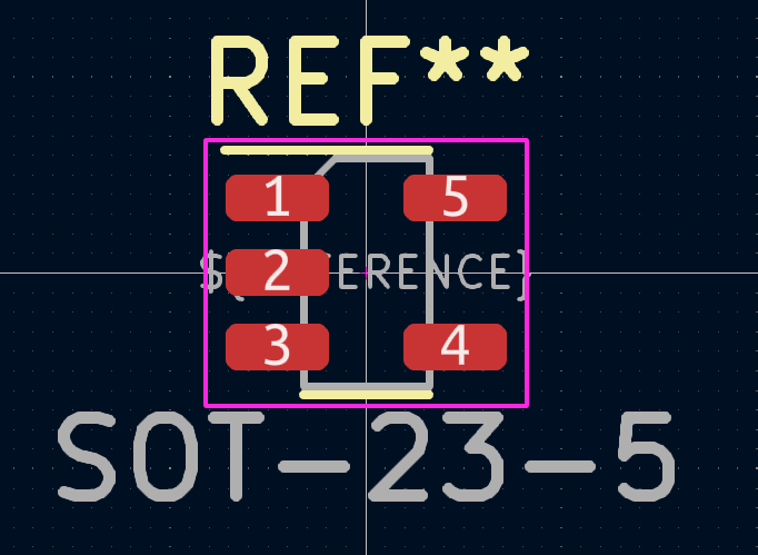
The areas in red are called pads and is where the component will interface with the board. The pads are then connected to each other to create a functional layout. In this image the pale yellow is silkscreen, meaning it will be printed on the board. The Pink is the courtyard and the grey is in the user/drawing layer and is only there to carry information to the designer. The courtyard's function is to make sure you don't pack components to tight. Overlapping the courtyards of two components will generate a warning or an error so you can fix it. The numbers on the pads are the pin numbers and correspond to the same numbers that you see on the symbols in the schematic. This is a place to be a bit careful. There is a standard way to number most generic footprint, but it is not a guarantee. This is the easiest place to mess up a design so make sure to at least triple check this! The correct pinning for your components should be found in the datasheet for the component.
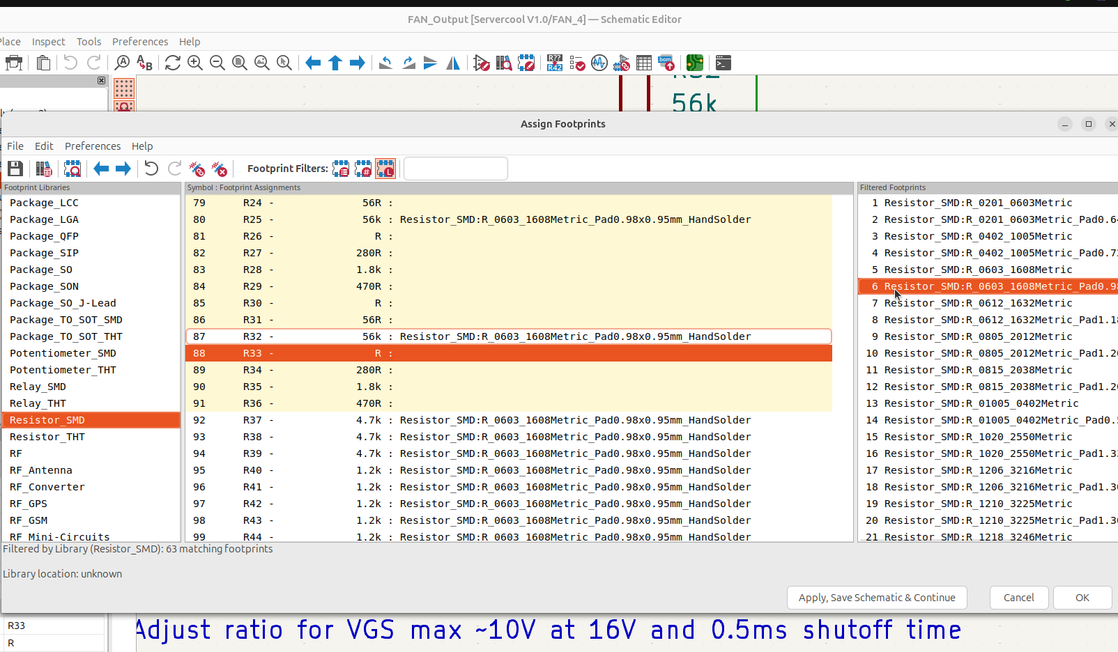
Assigning reference designators and footprints
Assigning footprints to symbols is done in the schematic editor in KiCAD. Open it and navigate to the footprint assignment tool. It is possible the program will ask you to assign reference designators if all components does not have those yet. If ask, say yes as it is required. The designators are the small "labels" that identify each schematic component uniquely. They are generic, such as "R?" for each resistor when placed. Assigning designators change the "?" for a number so your resistor is called "R1" instead.
A simple list simple list should now open. This list has all component listed, with an empty space for most if not all footprints. This list need to be filled with a valid footprint for each component. The component will be sorted in order so that similar components should be grouped together. Select the first component on the list. It should be highlighted in the schematic once you select it. Available footprints are listed in the list to the right where you can navigate to the correct footprint by selecting from categories. Once you have found your footprint, find it in the list and double click it. If the same should be used for the next component you can double click it and continue assigning. Continue until the list is completed.
Choosing a footprint
Which footprint will be the correct one is hard to say in a blog post. For specialized ICs, transistors and diodes it is usually listed in the datasheet. For resistors, capacitors and LEDs there is a bit more freedom to choose as you usually don't choose the exact component in the schematic stage, just the "specification". Resistors size is determined by the power rating, capacitors will be decided by the combination of voltage and capacitance it has. If it should be surface mount or through hole is also a choice that is dependent on taste, availability and space constraints. I usually only do surface mount, and avoid packages smaller than 0603. It is possible to hand solder 0402 but it is a pain to do. For a beginner, I would use 0805 for caps/resistors and similar or larger sizes for everything else if I wanted SMD, or through hole for easier soldering.
Place components cont'd
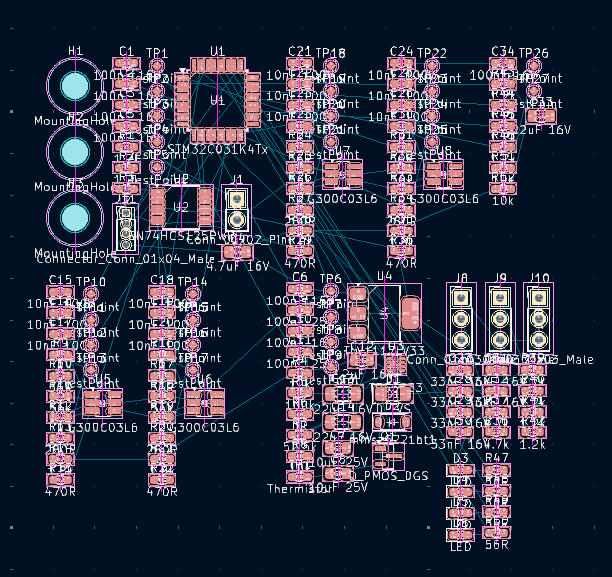
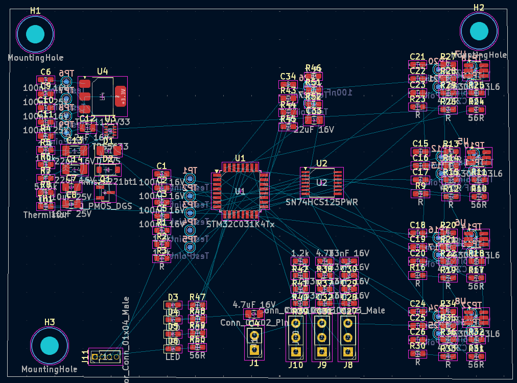
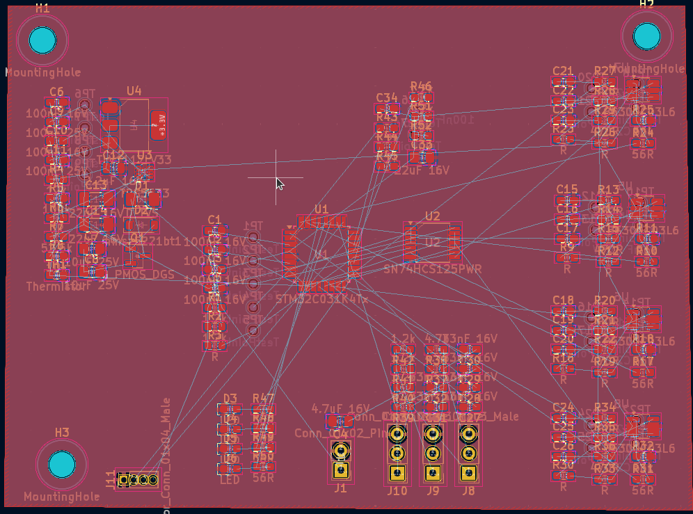
Now that all component has footprints you can start with the layout work for real. Press the "Update PCB with changes from schematic" button. Now a bunch of components should have shown up to be placed. These will be in a strange order, but we do not care about that just yet. Place the component somewhere in the middle of the screen. What you now have is something called a rats nest and for obvious reasons. The white lines show which pads should be connected and they are all over the place. At this stage it is also a good idea to make a rough estimate of the needed PCB size by eyeballing how much space the components use.

Lets get organized!
It is time to organize this mess into something more workable, by once again breaking it down into smaller blocks. Go back to the schematic editor and select all components that should be placed together. Once selected in the schematic they are also selected in the PCB editor. Move them to a space away from everything else. You can now either place them together manually or use Place->Auto-place footprints->Place Selected Footprints. Automatic placement and routing kind of suck as a general rule, but it is worth a try. If you are not happy with it, place them into blocks manually. Repeat until all components are placed into smaller "blocks". One thing that can save time here is to install the replicate layout plugin if you use KiCAD. It is an amazing plugin that allows you to place/route one subsheet and then replicate your work for all equal subsheets.

Create foundations of a board
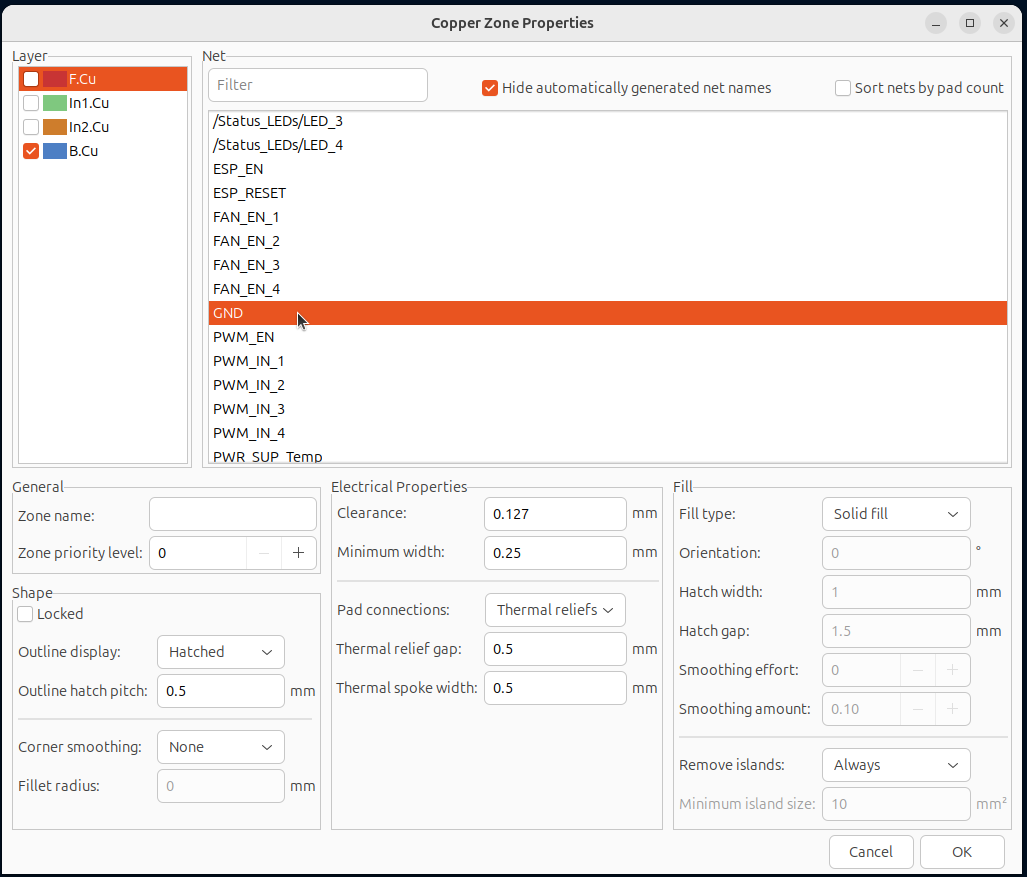
The blocks you just made can now be moved closer together. While doing this, try to place them in a way that makes sense. Powersupply stuff together, MCU in the middle and inputs/outputs somewhere together. Once this is done you can start with the outline. Select the edge cuts layer from the layer list. Use the crosshair to make a rough outline of the board where all components fit. At this point I do not bother with keeping the edges straight, just good enough. Make sure the shape is closed, or KiCAD will complain. Once this is done I also like to place a ground pour to get rid of a bit of the ratsnest. A friend of mine hinted that it might be a good idea to first route the ground "traces" as well to get an idea of how ground current will flow in the ground plane. This is important for boards with higher performance need. For this guide I will however assume that is not relevant and do a ground pour as it is easier. Place a ground pour on both layers by pressing add a filled zone. A dialogue will pop up. Choose GND and check the boxes for both layers. You will now place corners of a polygon. Place on in each corner of the outline for a complete ground pour. Now for a very important part. Place holes for screws or other mounting hardware before you start placing components and traces.

Layout
Now to the really fun part, starting to create a layout. Creating a layout is an iterative activity where it is always possible to do better. In other words, it is never "done" and at some point one just need to say stop and go for it.
Start by placing things that are sensitive to placement. Connectors, buttons, Indicator LEDs that need to fit into holes etc. Make sure to do this properly, it sucks to complete a layout and see that a connector was placed 2mm to far to the left and the re-do half the layout. Once this is done I like to start with power supply as usual. The power supply is usually one of the more important parts to get correct, or you will face problems with stability and/or EMI. The datasheet is usually a good resource for layout examples and guidelines.
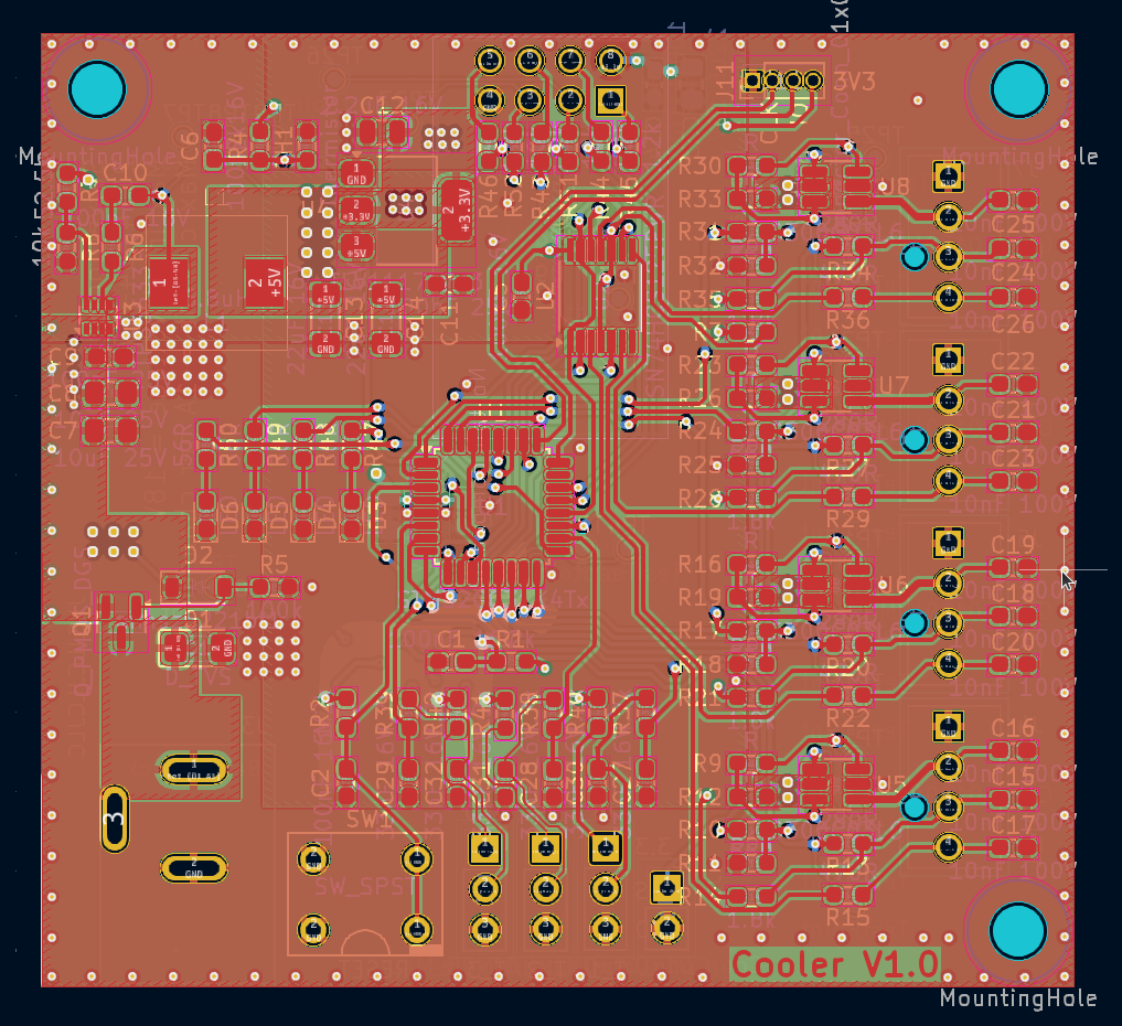
I understand that the step between "start layout" to the image above looks like that meme for how to draw an owl. But there is not much to say apart from "try and try again". Practice makes perfect.
Layout principles
Layout is in some way super simple, but also very, very hard to do "correctly". How much correctness matters is project dependent. As a general rule, the faster signals are the more important it is, and analogue signals more sensitive than digital ones. You will also notice that the "rules" are often in direct competition with each other. Knowing when to follow and when to bend the rules is something that comes with experience.
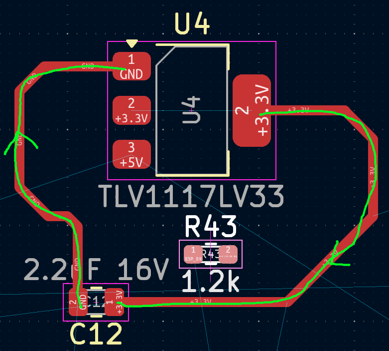
Keep current paths short
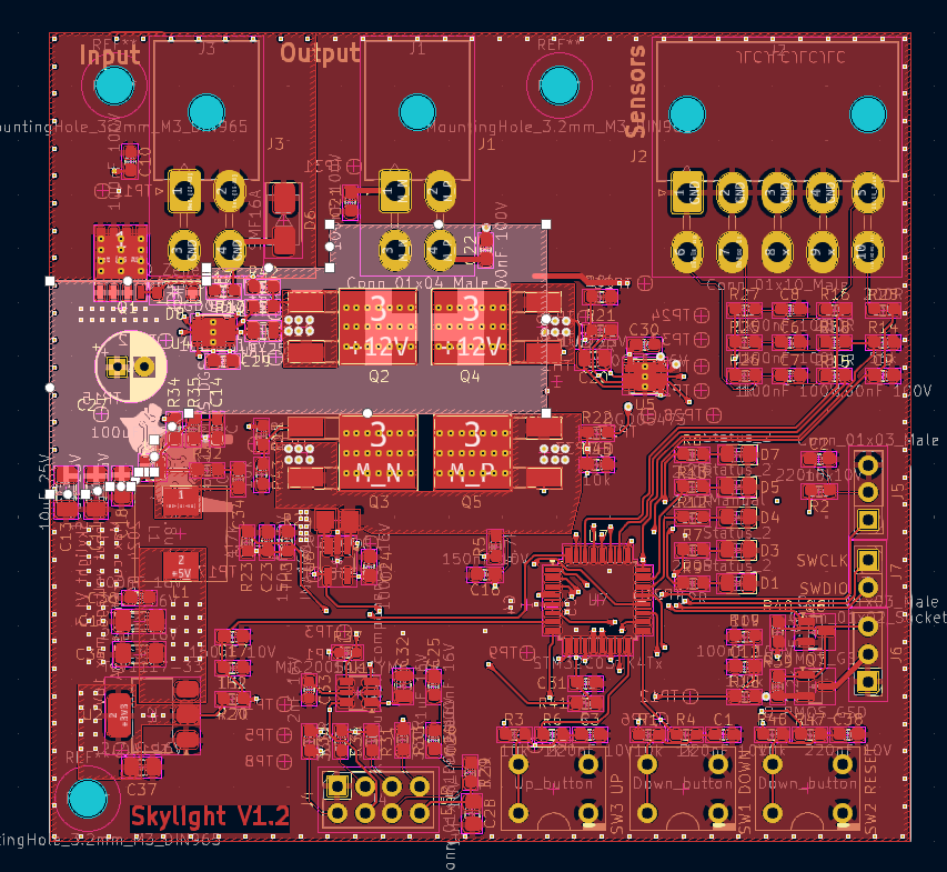
This one is rather self explanatory. Try to keep current paths as short as possible. This will make ohmic losses and parasitic inductance/capacitance to a minimum. This has benefits for power loss and signal distortion. The rule gets more and more important as current and signal speed increases. The board images is of a board that should be able to carry some 8 - 10A. The high current parts are in the top left quadrant.
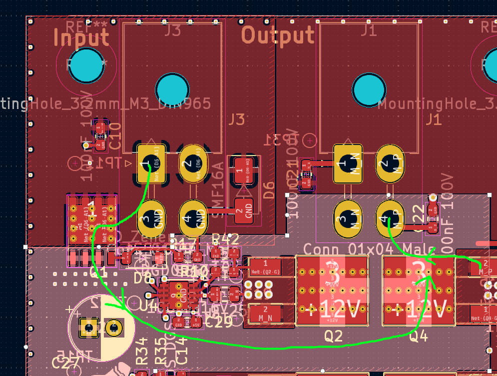
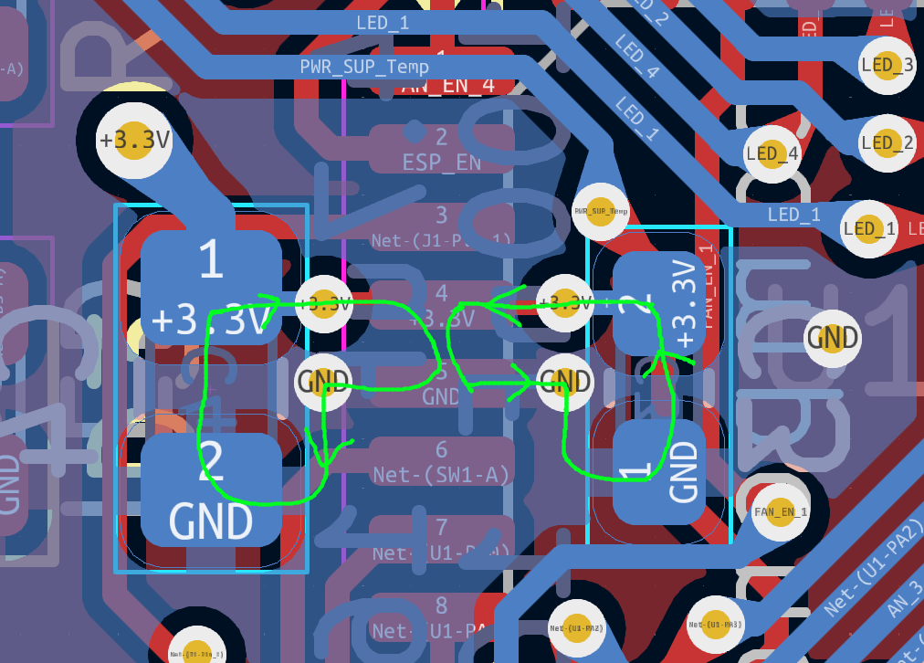
Keep current loops small
This one looks very similar to the first rule, but it is slightly different. Current always flow in a loop. From source, to load and back to the source again. When the magnitude of current changes, there is always some energy being lost into electromagnetic radiation, which in most designs is a bad thing. The magnitude of the radiative power is proportional by the area enclosed by the current loop. A small area mean less radiative power. For hobbyists, this usually only matters for power supplies and decoupling capacitors. Ideally, your first design should be a project where violating this rule is not catastrophic.
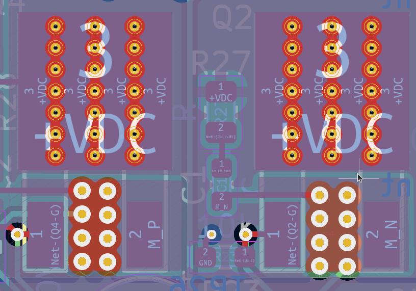
Heat management
Managing heat is a big part of PCB design. Even a relatively cool board might have spot sources of high power density that need to be managed. If your experience of thermal management comes from computers you might think that "thermal management" mean heatsinks. This is not necessarily the case. The heat needed to be dissipated are not so large usually, and a PCB is surprisingly good at spreading and dissipating heat. The copper sheet that builds up the conductive layers will spread the heat away from the component if you just let it. Breaks in the copper layer will limit the heat transfer so placing the component on a larger "zone" will help spreading the heat.
Another effective thing to do is thermal vias which mean that vias are placed for the purpose of conducting heat away to other layers that can assist spreading the heat more.
Good datasheets have design examples for thermal layouts. Read and understand these to help you with your design. You will also find information about how good you need to do this. This is the thermal information that is usually documented in the beginning of the datasheet
Silkscreen
The silkscreen is an easy part to miss, and it will be invaluable when it is time to build and debug your design. Make sure you mark as much as possible in the silkscreen layer. Silkscreen is free, apply accordingly! So make sure you mark
- Connector uses
- Polarity on connectors
- Indicator LEDs functions/names
- Name of the project
- PCB Version
- Date
- Rating for the board
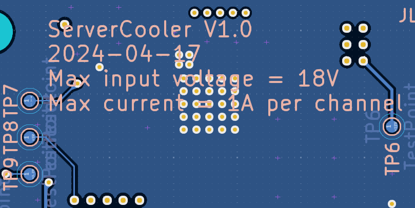
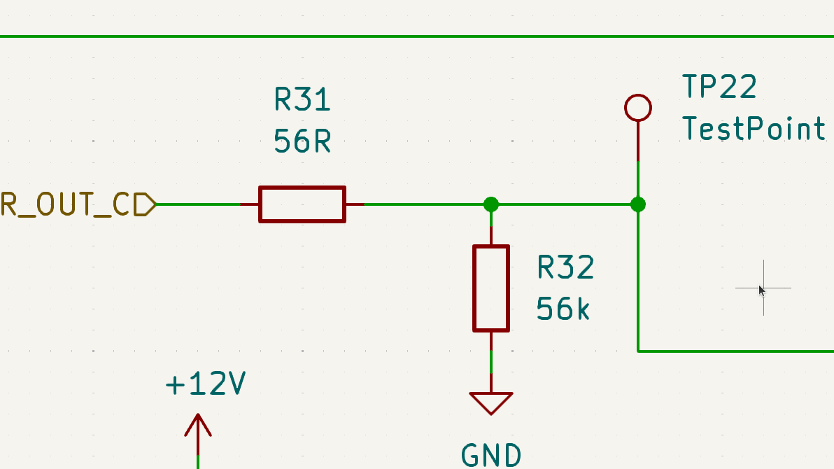
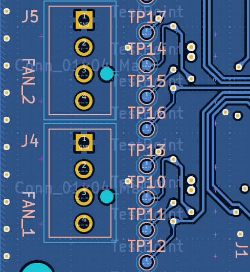
Test points
This is another part that is easy to forget. Make sure you place a LOT of testpoints. I try to fit on basically any internal signal that exist on the board as well as each net on the powersupplies. Remember, testpoints are free (expect board space) and NOT having one will make debugging annoying, so be liberal with them on prototypes!
Separation
Some parts need to be separated from each other. High current or fast signals will couple with surrounding traces and induce currents in these. Weak signals and especially weak analog signals can be affected by this. Because of this it is recommended that circuits with high dI/dt are routed far away from sensitive analogue circuits. For very sensitive sensing there are entire books written about it, but if you need to care about this you are not reading this post. For now, do not run a sensitive analog signal underneath your high power PWM trace.
Balance copper
This one is not important from an electrical perspective, but it is important for manufacturability of your board. Very shortly explained, the accuracy of plating/etching steps are affected by copper "balance", where balance mean how much is present on different parts of the board. If the amount of copper is way off on a larger board you might end up with over/under plating and over/under etching on parts of the board.
Another thing that can happen on larger boards is that they warp if only the top/bottom has a copper plane. The warpage risk is proportional to size. For a 100*100mm board you can ignore this rule if you need to.
Last steps
Check your work
Now that the layout is completed there is not much left to do. Run the DRC tool a last time to see if there are any problem. Then inspect the board a few times. I prefer to hide as many layers as possible to make it easier to spot errors. For example, hide all copper etc when checking that the silkscreen looks alright. I also use the 3D render tool in KiCAD to spot problems like bad silkscreen or access/mounting problems for bulky components, like connectors
Make fabrication files and order
The last thing to do is to create the fabrication files. The standard exchange format is gerber files. Exactly how each manufacturer want you to set up the export varies, so make sure to check before you order. JLCPCB for example has guides for how to export with several software suites.
Wait for delivery and solder the board
The next post will talk about how to assemble your board. It is usually pretty fast to make the board so you won't have to wait long. JLC usually takes 1 - 3 days depending on board setup + shipping.