Cooling my serverspace - Electronic hardware
Let's talk electronic hardware!
First of all, since this project is finished i will not go into much detail about the mistakes made. But the final hardware used and talked about is the third one.
Introduction
The hardware is easiest to understand if understood as a few blocks. After the block diagram is understood, further explanation of the hardware will make more sense. The block diagram over the hardware looks like this

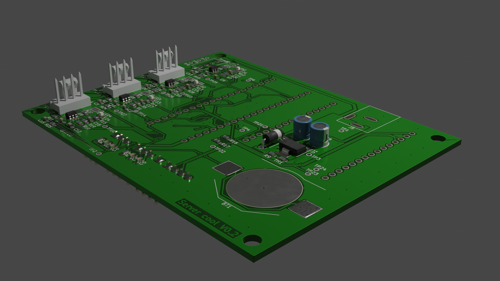
Schematic
Power supply

The power supply is a natural place to start the hardware design and analysis. The fans require a few 100mA of current each. With 4 fans I am planning to design it for about 2A of 12V or so. The next component is a 3.3V regulator to provide the STM32 board and the ESP with a stable 3.3V power rail. The regulator is a TLC1117 3.3V regulator from Texas Instruments. The components around it is more or less taken directly from the datasheet. Because of the predicted heat dissipation, a NTC is placed close to the supply to monitor the temperature. The powersupply is quite simple and wasteful, a fact that will be quite evident later on.
Temperature inputs

The next part to look at is the input for the temperature sensors. The inputs look a bit strange because I want to make them a bit more flexible than what a purpose built NTC input does. The idea is to be able to use a one wire sensor such as the ds18b20. In NTC mode, the NTC need to have a voltage divided built into whatever it is mounted on and C5 populated. In the case of a one wire sensor, C5 is depopulated or replaced with a much lower value for ESD protection. R3 is used as a short circuit protection. In the case of applying higher that 3.3V to pin 2, it should be possible for the controller to survive as the current is limited to what the clamping diodes in the microcontroller can withstand. C6 is used to stabilize the analogue input when operating in analogue mode. It is not needed for one wire and should be depopulated. 33nF is pretty large for the stabilization, but I wanted to have fewer different parts to place. The consequence of the large value for C6 is that the cutoff frequency will be quite low, but it will not matter for the application.
Fan drivers

The fan outputs has one power line, one ground return and two signal wires. The power output is a small high side load driver used to completely disconnect 12V when the fan is disabled or configured as not in use. The output is capable of driving around an ampere of current. The switch is based on the FDC6330L IC. It is a quite simple chip that in essence is a PMOS and an NMOS connected to provide a logic level, non inverting high side driver in a single component with minimal support parts. Two discharge resistors (R26 and R28) and a slew rate control capacitor (C14) are the only support components needed. C21 is there as a ESD protection capacitor.
The signal line are one one PWM control pin and one PWM feedback signal. The design of the signal IO is based on the specification for PWM fans. Noctua has a great whitepaper with information how to implement a control circuit that can be found here.The PWM control pin is connected directly to a push-pull configured GPIO on the microcontroller. Due to the direct connection, a short circuit limiting resistor R29 is provided, with a solder bridge in parallel in case it turns out the resistor solution is unworkable.
The last part is the PWM FB signal. It is pulled to 3.3V on the board through a current limiting pull-up resistor. A series resistor to provide short protection to the microcontroller is also in the design.
There is an inherent flaw in this design and that is the use of 3.3V control/feedback logic. It is tested to work with my intended fans, but it is technically out of spec. I have found at least one fan at home that will not start when 3.3V is used as a control signal. A future edition might include improvements to resolve this, but I let it be for now.
Layout
Powersupply

I'll be honest. This is the first time in about two years that I check this PCB. And well, it is not very well made now with the experience I have gained. It works, but looks kind of dodgy. Anyway. The main concerns for the power supply layout are
- The capacitors must be close to the regulator
- Thermal dissipation
- Close contact between the thermistor and device
The capacitors are simply placed close to the two terminals on the regulator. They each has a power plane connecting the components together. The ground connections are provided on the mostly solid ground plane on the underside of the board. Thermal dissipation is a great concern with this design. At the rated current consumption of about 200mA, the regulator dissipates close to 2W. This is not much, but it is not nothing either. Thermal vias are used to connect the large 3.3V zone to a larger zone on the bottom layer. The bottom layer zone does not need to have this size for electrical reasons, it is there to provide more area to dissipate heat.
Fan output

The fan outputs does not have that many constraints on the layout. There are no really high frequency signals and no high power devices to keep cool. The constraints are simply to make it fit and easy to assemble. The image show one of the outputs. A common 12V trace along the left edge is used to provide power for all of the outputs through the high side switch U9. I have tried to keep the components for the high side switch close to it as would be good practice. LED4 can also be seen here. LED4 does not have a functional purpose but is great for debugging.
Stay tuned for the next part, where software will be discussed!